Micro-and nano-structuring of materials with ultrashort pulses, with applications in astrophotonics, biosensing and organ-on-chip
principal investigators
senior investigators
phd students
Publications
Projects related
| Publications related (most relevant) | Appl. Surf. Sci. 436, (2018), J. Light. Tech. 37, (2019), Phot. Res. 8, 257 (2020), Prog. Quant. Electron. 72, 100266 (2020), Adv. Photon. Res. 2, (2021), Nature Photonics 17, 59 (2023) |
| Projects related | National (PID2020-119818GB-I00, PID2020-119003GB-I00, FIS2017-87970-R), Regional (SA136-P20, SA287P18) |
| Theses | Three defended, two in progress |
The unique way in which ultrashort pulses of high-intensity laser light interact with solid targets has opened a thriving field of research in the last decades with countless applications in optical and photonic manufacturing technologies. On one hand, using such pulses makes it possible to create controlled periodic nanostructures on the surface of many materials, thus modifying their surface properties on unprecedented spatial scales. On the other hand, in transparent materials such as glass and optical crystals, the refractive index of the material can be controlled at a micrometer scale, paving the way for the 3D manufacturing of integrated photonic microdevices that, in turn, allow us to control and spatially structure the light propagating through them. For over two decades, researchers from USAL have been working on refining these techniques and their applications.
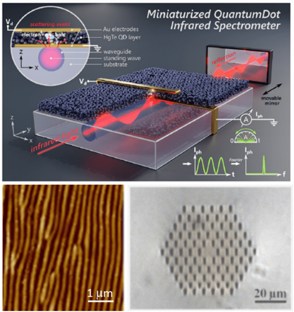
In recent years, efforts have primarily focused on two lines of work. Regarding the microstructuring of photonic devices, the unit has established itself internationally as a leading group in the integration of waveguides into state-of-the-art transparent crystals. This has led to the development of multifunctional active devices that leverage the excellent properties of these materials. The main application areas for these devices include astrophotonics, where ultra-compact quantum dot spectrometers have been developed in collaboration with ETH Zurich and the European Space Agency [Nature Photonics 17, 59 (2023)], and integrated lasers, achieving ultra-efficient devices [Prog. Quant. Electron. 72, 100266 (2020)]. Current efforts are directed towards incorporating these devices into Organ-on-Chip systems, where they can function as biosensing or control systems, assisted by 2D surface materials.
In the field of surface nanostructuring, in close collaboration for a decade with researchers from the Blas Cabrera Institute of Physical Chemistry and the Institute of Structure of Matter of the CSIC, among others, strategies have been developed to obtain regular surface patterns in the nanometer range in various polymeric and polymer matrix composite materials. This has been achieved using both nanosecond-range pulsed lasers and ultrashort pulses. As a result, processed surfaces are functionalized or enhance pre-existing properties, such as mechanical, chemical, optical, biocompatibility, etc., with applications in biomedicine, sensing, and surface engineering in general [J. Prada-Rodrigo et al. Opt. Laser Technol., 159 (2023); R. Rodriguez-Beltrán., Polymers 14, 5243 (2022)].